In the realm of advanced materials science, few techniques rival the precision and potential of Molecular Beam Epitaxy (MBE). This sophisticated process allows scientists to construct materials with atomic-level accuracy, opening doors to innovations that were once confined to the realm of science fiction. Let's embark on a journey into the world of MBE, exploring its intricacies, applications, and the profound impact it's having on technology and scientific research.
The Essence of Molecular Beam Epitaxy
At its core, Molecular Beam Epitaxy is a method of growing crystals with extraordinary precision. The name itself provides insight into the process:
- Molecular: We're dealing with individual molecules or atoms.
- Beam: These molecules are directed in controlled beams.
- Epitaxy: The process of depositing a crystalline layer on a crystalline substrate.
Imagine having the ability to paint with atoms, carefully layering them to create precise structures at the nanoscale. This is essentially what MBE allows scientists and engineers to achieve.
The Intricate Dance of Atoms
The MBE Process Unveiled
The MBE process begins with a carefully prepared substrate – the foundation upon which the crystal will grow. This substrate is heated to temperatures ranging from 500°C to 850°C (932°F to 1562°F), creating an ideal environment for crystal growth.
Next, beams of atoms or molecules are fired at the heated substrate. These beams are generated by effusion cells, often referred to as "atom guns." Each cell contains a different material and can be controlled independently, allowing for precise manipulation of the crystal's composition.
As these atoms settle on the surface, they form ultra-thin layers. The process is repeated, building up the desired crystal structure one atomic layer at a time. This level of control allows for the creation of structures that would be impossible to achieve through any other method.
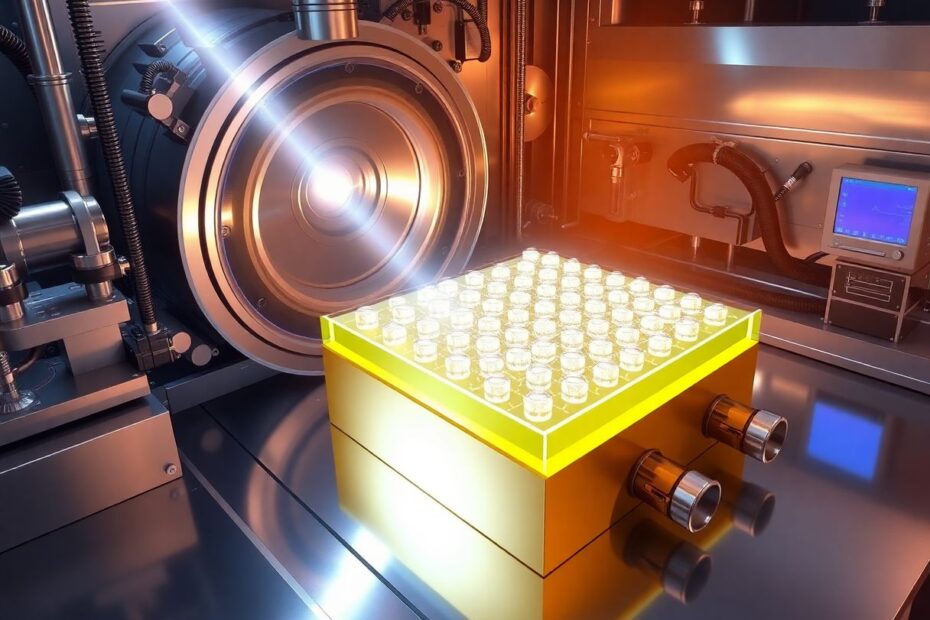
The Crucial Role of Ultra-High Vacuum
One of the most critical aspects of MBE is the ultra-high vacuum (UHV) environment in which the entire process occurs. This vacuum is so extreme that it approaches the pressure found in outer space – typically around one hundred trillionth of atmospheric pressure.
But why is such an extreme vacuum necessary? There are several crucial reasons:
Cleanliness: The UHV environment ensures that no stray particles interfere with the crystal growth process. Even a single dust particle could disrupt the delicate atomic structure being formed.
Mean Free Path: In UHV, atoms can travel from the effusion cells to the substrate without colliding with other particles. This ensures precise control over the deposition process.
Purity: Any contamination could ruin the crystal structure, so UHV is essential for maintaining material purity.
The importance of this vacuum cannot be overstated. It's akin to trying to paint a masterpiece in a dust storm versus in a perfectly clean studio. The UHV environment provides the "clean studio" necessary for atomic-level precision.
The Art and Science of Crystal Growth
Growing crystals with MBE is a delicate balance of art and science, requiring both technical expertise and a nuanced understanding of material behavior.
Precision in Time and Temperature
The growth rate in MBE is remarkably slow, typically only a few microns (or fractions of microns) per hour. This glacial pace is necessary for maintaining atomic-level control. Each layer is deposited with extreme precision, allowing for the creation of complex structures with specific properties.
Temperature control is equally crucial. Both the substrate and the effusion cells must be maintained at very specific temperatures. Even small fluctuations can affect the crystal's growth and properties.
Beam Control and Monitoring
The intensity and timing of each molecular beam must be carefully managed. This is achieved through sophisticated control systems that can adjust the beams in real-time based on the crystal's growth.
Advanced monitoring equipment, including reflection high-energy electron diffraction (RHEED) systems, allow scientists to observe the crystal growth in real-time. This enables adjustments to be made on the fly, ensuring the highest possible quality in the final structure.
Applications: Where MBE Shines
The precision afforded by MBE makes it invaluable in a wide range of applications, particularly in fields requiring advanced materials with specific properties.
Semiconductor Lasers
MBE has revolutionized the development of semiconductor lasers, which are used in a variety of applications including:
- Fiber optic communications
- CD and DVD players
- Laser pointers
- Medical devices
The ability to precisely control the composition and thickness of semiconductor layers allows for the creation of lasers with specific wavelengths and efficiencies.
High-Speed Electronics
In the realm of high-speed electronics, MBE-grown materials are pushing the boundaries of what's possible. Ultra-fast transistors and other components created through MBE are enabling the development of next-generation computing and communication technologies.
Advanced Solar Cells
MBE is at the forefront of developing more efficient photovoltaic materials. By creating precise multi-junction solar cells, researchers are able to capture a broader spectrum of light, significantly increasing energy conversion efficiency.
Quantum Devices
Perhaps one of the most exciting frontiers for MBE is in the field of quantum devices. The atomic-level precision of MBE is crucial for creating the delicate structures required for quantum computing and sensing technologies.
Optoelectronics
MBE plays a vital role in creating devices that interact with both light and electricity. This includes advanced LEDs, photodetectors, and integrated optical circuits.
Advantages and Challenges
The Power of Precision
The unparalleled control over material composition and structure is MBE's greatest strength. This precision allows for:
- Creation of materials with tailored electronic and optical properties
- Development of novel heterostructures and quantum wells
- Exploration of new material combinations and properties
Purity and Flexibility
The ultra-high vacuum environment ensures extremely clean material growth, resulting in high-purity crystals. Additionally, MBE can work with a wide range of materials, from semiconductors to metals and even some organic compounds.
Real-Time Monitoring and Low-Temperature Processing
The ability to observe and adjust growth in real-time is a significant advantage of MBE. Furthermore, compared to some other crystal growth techniques, MBE often allows for lower temperature processing, which can be crucial for certain materials.
The Hurdles to Overcome
Despite its power, MBE does face some challenges:
Cost: MBE equipment is extremely expensive to purchase and maintain, often costing millions of dollars.
Speed: The slow growth rate makes it less suitable for large-scale production.
Complexity: Operating MBE systems requires highly skilled personnel and careful process control.
Material Limitations: Not all materials are suitable for MBE growth, limiting its applications in some areas.
The Evolution of MBE: From Theory to Practice
The journey of MBE from a theoretical concept to a cornerstone of advanced materials science spans several decades:
1958: Günther Leibfried and Nicolas Cabrera lay the theoretical groundwork for controlled crystal growth.
1960s: Early experiments with vacuum evaporation techniques pave the way for MBE.
1968: Alfred Y. Cho and John R. Arthur Jr. at Bell Labs develop the basic MBE technique, marking a pivotal moment in materials science.
1970s: Rapid advancement of MBE technology and understanding, with researchers exploring its potential across various materials.
1980s-present: Continuous refinement of MBE capabilities, expanding its applications and improving control and monitoring systems.
MBE in Perspective: The Ultimate 3D Printer
To grasp the essence of MBE, consider it as the world's most precise 3D printer:
- Instead of plastic filament, it uses beams of atoms.
- Rather than printing layer by layer, it builds atom by atom.
- The "print bed" (substrate) is heated to ensure the atoms stick in the right places.
- The "printing" happens in a vacuum chamber cleaner than any cleanroom on Earth.
While a home 3D printer might take hours to create a small object, an MBE machine could spend that long creating a layer thinner than a human hair – but with atomic-level precision that's unmatched by any other manufacturing process.
The Future of MBE: Pushing the Boundaries of Science and Technology
As we look to the future, MBE is poised to play an increasingly important role in pushing the boundaries of what's possible in materials science and technology.
Quantum Computing Revolution
The development of practical quantum computers relies heavily on the ability to create precise, pure materials with specific quantum properties. MBE's atomic-level control makes it an ideal technique for creating the complex structures needed for quantum bits (qubits).
Next-Generation Solar Cells
As the world seeks more efficient and sustainable energy sources, MBE is at the forefront of developing ultra-high-efficiency solar cells. By creating precise multi-junction cells and exploring new material combinations, researchers aim to push solar energy conversion beyond current limits.
Advanced Sensors and Detectors
MBE-grown materials are enabling the development of ultra-sensitive detectors for applications ranging from medical imaging to environmental monitoring. The ability to tailor material properties at the atomic level allows for unprecedented sensitivity and specificity.
Novel Materials Exploration
Perhaps most excitingly, MBE opens up the possibility of creating entirely new materials with properties that don't exist in nature. By exploring new combinations of elements and precise structural arrangements, scientists may discover materials with revolutionary capabilities in areas like superconductivity, magnetism, or optical properties.
Conclusion: The Atomic Architect's Ultimate Tool
Molecular Beam Epitaxy represents the pinnacle of precision in material science, allowing us to arrange atoms like building blocks and create structures that nature never imagined. While it may never be a high-volume production technique, MBE's ability to create ultra-pure, highly controlled crystal structures makes it an invaluable tool for pushing the boundaries of what's possible in electronics, photonics, quantum technologies, and beyond.
As we continue to explore the nanoscale world, MBE stands as a testament to human ingenuity – a way to paint with atoms and sculpt with molecules, creating the technologies of tomorrow, one atomic layer at a time. Its impact on fields ranging from telecommunications to renewable energy to quantum computing underscores its importance in shaping our technological future.
The journey of MBE from a laboratory curiosity to a cornerstone of advanced materials research highlights the power of precision and control in scientific endeavors. As we look to the challenges and opportunities of the 21st century, techniques like MBE will be crucial in developing the materials and technologies needed to address global issues and push the boundaries of human knowledge.
In the end, Molecular Beam Epitaxy is more than just a technique for growing crystals – it's a gateway to a world of possibilities at the atomic scale, where the limits of what we can create are bounded only by our imagination and our ever-expanding scientific understanding.